top of page

SE-5AT Semiconductor Series|Optical Inspection
Intelligent optical wafer/chip surface defect and height detection equipment
Wafer Inspection Technology
Advantages and Features
高精度表面瑕疵檢測,AI智慧判讀加值解決方案
本光學檢測設備專為各類平面式載體材料設計,整合高解析成像模組與AI視覺辨識演算法,能快速精準地偵測異物(Particle)、刮傷、孔洞等表面瑕疵,適用於晶圓檢查、光罩檢測、SIC晶片及透明載體等高標準應用場域。支援線掃與面陣鏡頭選配,涵蓋低倍率到高倍率觀察需求,搭載紅外線自動對焦技術,亦能穩定對應透明與半透明材質。透過AI深度學習、影像相減與灰階比對演算,本設備不僅提升瑕疵檢出率,也具備優異的系統彈性與客製化潛力,適合導入於半導體製程、光電產線、高階材料品管等領域。
Advantages and Features
1 / 多倍率光學檢測模組
支援低倍率至高倍率鏡頭模組,依需求調整觀測尺度
2 / 紅外線自動對焦技術
提升對焦穩定性與透明物體檢測效率
3 / 透明材質支援
可有效檢測光罩、玻璃載體等高透光材料
4 / AI深度學習訓練模組
-
自建訓練模型與樣本資料庫,實現高準確率檢測分類
-
可持續優化與學習新型瑕疵
5 / 影像相減檢測法
有效針對微小差異進行比對與標記,適用於穩定性高的批量生產監控
Automatic optical testing equipment specifications
設備
面陣規格
項目 | 規格A | 規格B |
|---|---|---|
崩邊 | 30um*30um以上 | 3um*3um以上 |
異物 | 30um*30um以上 | 3um*3um以上 |
刮傷 | 最小線寬30um | 最小線寬3um |
髒污 | 30um*30um以上 | 3um*3um以上 |
備註1 | 成像精度10um,檢出為3pixel以上 | 成像精度1um,檢出為3pixel以上 |
備註2 | 粉塵亦會被檢出,設備包含靜電噴槍去除粉塵元件 | 粉塵亦會被檢出,設備包含靜電噴槍去除粉塵元件 |
備註3 | - | 主要針對小型化的瑕疵為主 |
Image Detection
Measurement interface

AI judgment results clearly show the defect type, coordinates, area, and quantity on the wafer, and the data is fully integrated


Chip mapping defect detection screen
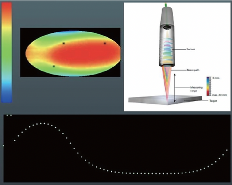
Laser Sensor
bottom of page